![]({"xsmall":"https://www.zeiss.co.jp/content/dam/rms/countries/singapore/apac/top-lowkv.png/_jcr_content/renditions/original.image_file.100.100.file/top-lowkv.png","small":"https://www.zeiss.co.jp/content/dam/rms/countries/singapore/apac/top-lowkv.png/_jcr_content/renditions/original.image_file.360.360.file/top-lowkv.png","medium":"https://www.zeiss.co.jp/content/dam/rms/countries/singapore/apac/top-lowkv.png/_jcr_content/renditions/original.image_file.768.768.file/top-lowkv.png","large":"https://www.zeiss.co.jp/content/dam/rms/countries/singapore/apac/top-lowkv.png/_jcr_content/renditions/original.image_file.1024.1024.file/top-lowkv.png","xlarge":"https://www.zeiss.co.jp/content/dam/rms/countries/singapore/apac/top-lowkv.png/_jcr_content/renditions/original./top-lowkv.png","xxlarge":"https://www.zeiss.co.jp/content/dam/rms/countries/singapore/apac/top-lowkv.png/_jcr_content/renditions/original./top-lowkv.png","max":"https://www.zeiss.co.jp/content/dam/rms/countries/singapore/apac/top-lowkv.png/_jcr_content/renditions/original./top-lowkv.png"})
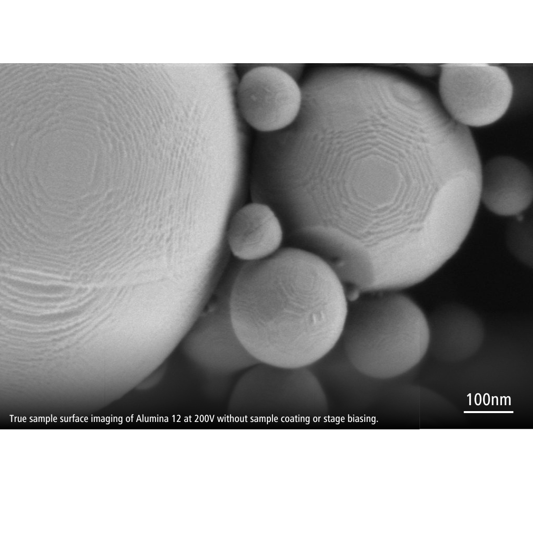
低加速電圧および極低加速電圧で真の試料表面イメージングを達成
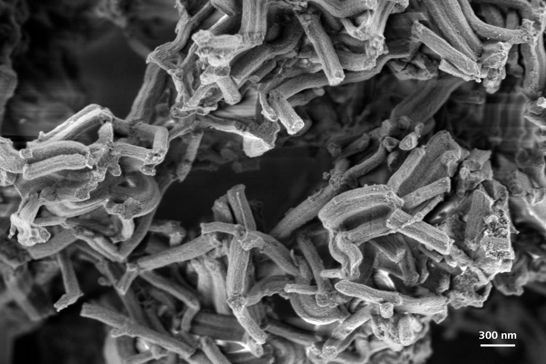
ZEISS Gemini 3 カラムで実現
非導電性試料や磁性体試料の真の表面情報を明らかにするため、これらの試料を表面コーティングなしで高分解能でイメージングすることが求められています。
高い分解能で真の試料表面のイメージングを実現するためには、低加速電圧の使用が望ましいですが、低加速電圧または極低加速電圧でのSEMイメージングには、以下の課題があります:
(i) SN比が低い
(ii) 分解能が低い
(iii) 電子ビーム調整不足による画像の歪み
ZEISS Gemini 3 カラムで相乗的に機能する新しいSmart Autopilot(新しい電子光学エンジン)とナノツインレンズを組み合わせることで、どのようにして低加速電圧または極低加速電圧で、非導電性試料や磁性体試料表面の高分解能イメージングが可能になるのかをご紹介します。
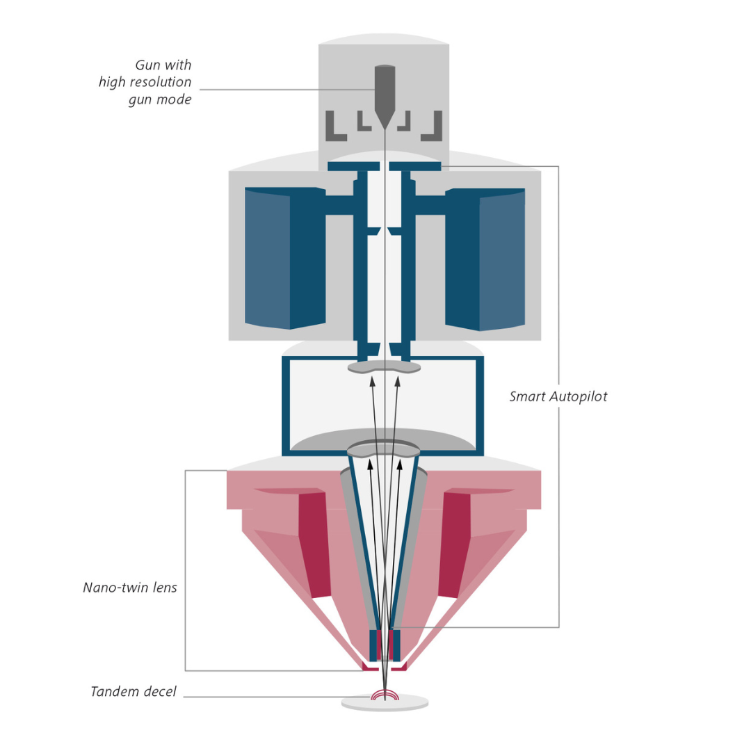
![]({"xsmall":"https://www.zeiss.co.jp/content/dam/rms/countries/singapore/apac/geminicolumn.png/_jcr_content/renditions/original.image_file.100.100.file/geminicolumn.png","small":"https://www.zeiss.co.jp/content/dam/rms/countries/singapore/apac/geminicolumn.png/_jcr_content/renditions/original.image_file.360.360.file/geminicolumn.png","medium":"https://www.zeiss.co.jp/content/dam/rms/countries/singapore/apac/geminicolumn.png/_jcr_content/renditions/original.image_file.768.768.file/geminicolumn.png","large":"https://www.zeiss.co.jp/content/dam/rms/countries/singapore/apac/geminicolumn.png/_jcr_content/renditions/original.image_file.1024.1024.file/geminicolumn.png","xlarge":"https://www.zeiss.co.jp/content/dam/rms/countries/singapore/apac/geminicolumn.png/_jcr_content/renditions/original./geminicolumn.png","xxlarge":"https://www.zeiss.co.jp/content/dam/rms/countries/singapore/apac/geminicolumn.png/_jcr_content/renditions/original./geminicolumn.png","max":"https://www.zeiss.co.jp/content/dam/rms/countries/singapore/apac/geminicolumn.png/_jcr_content/renditions/original./geminicolumn.png"})
Gemini 3 カラムの紹介
Gemini 3の光学系は、低加速電圧での分解能とコントラスト強化のために最適化されています。今では試料を電場や磁場にさらすことなく、1 kV未満でサブナノメートルイメージング可能です。低加速電圧から高加速電圧までのあらゆる観察条件下で最高の分解能を確保することができます。
Gemini 3は、相乗的に機能するナノツインレンズと新しい電子光学エンジンであるSmart Autopilotの2つのコンポーネントで構成されています。
ナノツインレンズにより、低加速電圧でも、サブナノメートルの分解能と優れた信号検出効率を実現します。ナノツインレンズは、標準的なGemini対物レンズと比較して、低加速電圧でのレンズ収差を大幅に低減し、Inlens検出器の信号が低加速電圧イメージング条件下で強化されます。
Smart Autopilotとナノツインレンズを組み合わせることで、ビーム収束角度をコンデンサレンズで最適化することにより、あらゆる観察条件で最高の分解能を実現します。
広視野オーバービューモードにより、試料ナビゲーションと高分解能イメージングのスムーズな切り替えができます。新しいオートフォーカス機能により、高速で最適な画質が実現します。