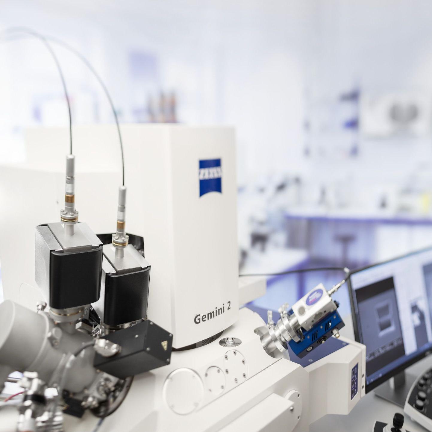
ZEISS Crossbeam
3D分析と試料作製を高いスループットで実現するFIB-SEM
イメージングと分析性能を兼ね備えた高分解能電界放出型走査電子顕微鏡(FE-SEM)に、次世代集束イオンビーム(FIB)の処理能力を統合しました。研究所などの複数のユーザーが利用する研究施設に最適です。ZEISS Crossbeamのモジュラープラットフォームなら、大量の材料アブレーションにLaserFIBを使用するなど、増大するニーズに合わせて既存システムをアップグレードできます。ミリング、イメージングや3D解析において、CrossbeamがFIB使用時の作業をスピードアップさせます。
TEMラメラ作製
NanoSQUIDSの結晶構造の観察


SEMで最大限の情報を獲得
- Gemini電子光学系を使った高分解能SEM画像から試料の正確な情報を抽出
- 2Dの表面敏感な画像や3DトモグラフィーでCrossbeamの優れたSEM性能を活用
- 低加速電圧においても高い分解能、コントラスト、S/N比を実現
- 様々な検出器を用いて試料の包括的な特性評価が可能。独自のInlens EsB検出器により純粋な材料コントラストが得られる
- 帯電アーチファクトに邪魔されることなく非導電性の試料を観察可能


FIBを使った試料作製のスループット向上
- インテリジェントなFIBスキャンで材料をより早く正確に除去し、加工時間を最大で40%短縮
- Ion-sculptor FIBカラムが新たなFIB処理の方法を実現。試料へのダメージを最小限に抑え、試料の質を最大限高めると同時に加工を高速化
- FIB分解能を損なうことなく、最大100 nAの電流を用いて試料を正確かつ迅速に操作可能
- TEMラメラ作製には、Ion-sculptor FIBの低加速電圧機能を使用。アモルファス化による試料のダメージを最小限に抑えつつ、極薄膜試料を実現


はんだの3Dトモグラフィー。本画像はイメージングとEDS分析を組み合わせたマルチモーダルなワークフローの一部。(画像幅38 µm)


FIB-SEM分析で最高の3D分解能を実現
- 統合された3D EDS と3D EBSD測定のメリットを活用
- ミリング、イメージングや3D解析において、CrossbeamはFIBを使った作業を効率化
- 業界をリードする高速かつ正確なトモグラフィーを提供するZEISS Atlas 5パッケージで、Crossbeamの性能を拡張
- Atlas 5の統合3D解析モジュールにより、トモグラフィー中にEDSやEBSD分析が可能
- 業界屈指の等方性ボクセルサイズと最高レベルの3D分解能を有するFIB-SEMトモグラフィーで優れた結果を取得。Inlens EsB検出器は、深さ3 nm未満の情報で、表面感度と材料コントラストの高い画像を取得可能
- ミリングしながら断面画像を収集し、トモグラフィーの所要時間を削減。撮像後にトラッキング可能な実ボクセルサイズの記録と、画質調整のための自動ルーチン群
Crossbeamファミリー


Crossbeamによるワークフロー
レーザー、TEMラメラ作製、相関クライオのワークフローを調整するためのガイド付きワークフローを活用ください
Crossbeamレーザーのワークフロー
深部にある関心領域に素早くアクセスし、マルチスケールで相関ワークフローを実行。大体積の分析で、深く埋もれた関心領域をより正確に取得します。EDSやEBSDなどの3Dイメージングや分析も可能です。半自動化装置により、時間の節約とスループットのさらなる向上が実現しました。
お手持ちの Crossbeamにフェムト秒レーザーを追加すれば、特定部位から超高速で試料を作製できます。FIB-SEMのチャンバーは清潔に保たれ、必要に応じて半自動化ワークフローで遠隔操作が可能です。
メリット:
- 深部にある内部構造に素早くアクセス
- 制御された真空環境でフェムト秒レーザーパルスを使用するため、ダメージと熱影響を最小限に抑える
- レーザー作業を専用チャンバー内で行うことで、FIB-SEMのメインチャンバーと検出器を汚染から保護
- レーザー処理、研磨、洗浄および集束イオンビームSEM用チャンバーへの試料の移動を自動化
- TEMラメラ上の断面からピラー配列まで、複数の試料を作製し、様々な材料にプリインストールされたレシピを使用して効率的に作業
-


銅マイクロバンプとフリップチップを相互接続したマルチチップパッケージ、レーザによる破砕と集束イオンビームによる研磨を施した横断面、トレンチ深さ1.6 mm。

銅マイクロバンプとフリップチップを相互接続したマルチチップパッケージ、レーザによる破砕と集束イオンビームによる研磨を施した横断面、トレンチ深さ1.6 mm。
1.素早いアクセス、最適化された作製、マルチスケール
- PFIB(プラズマFIB)よりも数段速く、深部にある構造が明らかに
- 制御された真空環境でフェムト秒レーザー処理を行うため、ダメージと熱の影響を受ける領域を最小限に抑える
- レーザー処理から集束イオンビームを用いた分析まで大気非暴露のワークフローを維持(環境ガスは窒素かアルゴンを選択)
- 調整済みワークフローで、すでに入手している3D X線顕微鏡またはその他の外部データセットと関心領域を相関させる
- 新しいバーストモードでアブレーションの速度とパフォーマンスを向上させる
-

LaserFIBの詳細、レーザーチャンバーとレーザー光学系(右)、収束イオンビームSEMチャンバー(左)。

LaserFIBの詳細、レーザーチャンバーとレーザー光学系(右)、収束イオンビームSEMチャンバー(左)。
2.ワークフローの自動化
- 自動化されたシャトリングおよびレーザー処理によって、LaserFIBで複数の試料を作製する時間が短縮し、スループットが向上
- システムを遠隔操作し、レーザー、電動搬送ロッド、さらにFIB-SEMを使用した無人自動実験が可能
- ソフトウェアを1回クリックするだけで、レーザーとFIB-SEMの登録が完了
- スクリプトによりワークフローの自動作成が可能になり、実験の効率がアップ
- スクリプトを使用すれば、複数のレシピの組み合わせや、真空条件(窒素またはアルゴンガス)の有効化が可能に
-

銅にレーザー処理で3つの溝を作成。クロスジェットを行わなかった部位(上)と行った部位(下)。

銅にレーザー処理で3つの溝を作成。クロスジェットを行わなかった部位(上)と行った部位(下)。
3.清潔さを保ち、スループットと使いやすさを確保
- レーザー作業を専用チャンバー内で行うことで、FIB-SEMのメインチャンバーと検出器を汚染から保護
- 保護ガラスウィンドウと高圧噴射法を活用。クロスジェット(窒素またはアルゴンのガス流)が、レーザー光学系の下の保護ガラスに対するアブレーションした材料の堆積を防ぎ、レーザー処理中も清潔な状態を維持
- レーザーは、特に複数部位の試料を作製する際に、溝の周囲に新たに堆積した材料を除去するのにも有用
-

シリコンの25のピラー配列(バーストモードで約30秒間レーザー加工し、ガリウム集束イオンビームで精密研磨された状態)。

シリコンの25のピラー配列(バーストモードで約30秒間レーザー加工し、ガリウム集束イオンビームで精密研磨された状態)。
4.試料作製の新たな世界を開く
- フェムト秒レーザーとガリウム集束イオンビームのメリットを組み合わせることで、巨大な横断面、TEMラメラおよびアトムプローブトモグラフィーの試料からピラー配列まで、幅広い試料を作製し、微細圧縮試験またはシンクロトロン顕微鏡検査およびナノCTを実施
- フェムト秒レーザーを用いて、幅および深さが最大ミリメートル単位の極めて大きな断面を加工
- 精密な深さのレーザー加工により、特定の材料層を除去
- プリインストールしたレシピを使用するか、ワークフローを個別に定義すれば、効率的なレーザー処理に適したパラメータを簡単に見つけることが可能


。Crossbeam 550")
。Crossbeam 550")
。Crossbeam 550")
。Crossbeam 550")
自動試料作製によって加工したTEMラメラ配列(ラメラ幅:約20 µm)。Crossbeam 550
自動試料作製によって加工したTEMラメラ配列(ラメラ幅:約20 µm)。Crossbeam 550
TEMラメラ作製用ワークフロー
TEMラメラの作製は、ほとんどのFIB-SEMユーザーにとって欠かせない作業です。ZEISSは、特定位置で作製するための自動ワークフローを提供し、これによって得られるラメラは、高分解能TEMおよびSTEMイメージング、原子分解能での分析に最適です。試料の関心領域に移動し、バルク試料から関心領域を含むTEMラメラを抽出してから、バルクミリングやトレンチングを行って、ピックアップと必要に応じて薄片化を行います。
-
への自動ナビゲーション")
1.試料の関心領域(ROI)への自動ナビゲーション
への自動ナビゲーション")
– 関心領域を探す手間をかけることなく、ワークフローを開始
– エアロックのナビゲーションカメラを用いて試料の位置を特定
– 統合ユーザーインターフェースにより関心領域に容易にナビゲート
– SEMのひずみのない広視野を活用1.試料の関心領域(ROI)への自動ナビゲーション
- ● 関心領域を探す手間をかけることなく、ワークフローを開始
- ● エアロックのナビゲーションカメラを用いて試料の位置を特定
- ● 統合ユーザーインターフェースにより関心領域に容易にナビゲート
- ● SEMのひずみのない広視野を活用
-

2.自動試料作製(ASP)によるバルク試料のラメラ作製

– 簡単な3段階の工程で作製を開始:ASP
– ドリフト補正、デポジション、ならびに粗加工および仕上げ加工などのレシピを定義
– FIBカラムのイオン光学系によりハイスループットのワークフローが可能に
– バッチの前処理を開始するためにレシピを複製し、必要なだけ繰り返すことが可能画像:ピックアップ直前の銅試料のラメラ。自動試料作製機能で作製。集束イオンビームによる作製およびイメージング。実視野:76.22 µm。
ピックアップ直前の銅試料のラメラ。自動試料作製機能で作製。集束イオンビームによる作製およびイメージング。実視野:76.22 µm。
2.自動試料作製(ASP)によるバルク試料のラメラ作製
- ● 簡単な3段階の工程で作製を開始:ASP
- ● ドリフト補正、デポジション、ならびに粗加工および仕上げ加工などのレシピを定義
- ● FIBカラムのイオン光学系によりハイスループットのワークフローが可能に
- ● バッチの前処理を開始するためにレシピを複製し、必要なだけ繰り返すことが可能
-

3.ピックアップ

– マイクロマニピュレーターの先端にラメラを付ける
– ラメラをバルクから切り出す
– その後、ラメラがピックアップ可能な状態となり、TEMグリッドに移すことが可能画像:ZEISS CrossbeamのTEMラメラ作製ワークフローの一部。TEMラメラが付いたマイクロマニピュレーターの針がバルクからピックアップされています。
ZEISS CrossbeamのTEMラメラ作製ワークフローの一部。TEMラメラが付いたマイクロマニピュレーターの針がバルクからピックアップされています。
3.ピックアップ
- ● マイクロマニピュレーターの先端にラメラを付ける
- ● ラメラをバルクから切り出す
- ● その後、ラメラがピックアップ可能な状態となり、TEMグリッドに移すことが可能
-

4.薄片化:最終ステップは、TEMラメラの品質を決定するため非常に重要

– 本装置は、薄片化のライブモニタリングで希望の厚さにできるように設計されている
– 2つの検出器シグナルを同時に使用してラメラの厚さを判断し、一方の検出器(SE検出器)で再現性の高い最終の厚さを得て、もう一方の検出器(Inlens SE検出器)で表面品質を制御する
– アモルファス化を最小にして、高品質の試料を作製する画像:仕上げの薄片化後のシリコン試料のTEMラメラ
仕上げの薄片化後のシリコン試料のTEMラメラ
4.薄片化:最終ステップは、TEMラメラの品質を決定するため非常に重要
- ● 本装置は、薄片化のライブモニタリングで希望の厚さにできるように設計されている
- ● 2つの検出器シグナルを同時に使用してラメラの厚さを判断し、一方の検出器(SE検出器)で再現性の高い最終の厚さを得て、もう一方の検出器(Inlens SE検出器)で表面品質を制御する
- ● アモルファス化を最小にして、高品質の試料を作製する
への自動ナビゲーション")
への自動ナビゲーション")


クライオ条件下でのTEMラメラ作製および三次元解析
クライオ顕微鏡では、生理的環境下に近い状態での細胞構造の観察が可能です。しかし、ユーザーは、試料作製、失透、アイスコンタミネーション、試料ロス、または複数のイメージング手法の相関といった複雑な課題に直面することになります。ZEISS相関クライオ顕微鏡ワークフローは、ワイドフィールド顕微鏡、レーザー走査型顕微鏡、集束イオンビーム搭載走査型電子顕微鏡をシームレスに組み合わせたソリューションです。ハードウェアもソフトウェアも、蛍光高分子の位置確認から高コントラストのクライオ電子線トモグラフィーイメージングおよびTEMグリッド状でのラメラ薄片化まで、相関クライオ顕微鏡ワークフローのニーズに合わせて最適化されています。
-

生理的環境に近い状態をイメージング
- ● マルチモーダルなイメージング手法を統合したシームレスなクライオワークフロー
- ● 失透やアイスコンタミネーションから試料を保護
- ● 高分解能蛍光イメージング
- ● 高コントラストボリュームイメージングと3D再構成
- ● クライオTEM使用時の標的オングリッドラメラ薄片化
- ● 極低温から室温まで幅広く応用可能
-

シンプルなワークフローで研究に集中
相関クライオ顕微鏡ワークフローは、クライオ条件下で様々なイメージング手法の組み合わせを簡単に操作できます。このワークフローソリューションは、光学・電子顕微鏡法を組み合わせ、効率的に3Dイメージング及びTEM試料作製を可能にします。専用アクセサリーによりワークフローが簡素化され、顕微鏡間で低温試料を安全かつ簡単に搬送できます。ZEISS ZEN Connectによって、全ワークフローのデータ管理が保証され、データがコンテキスト内に保存されます。更に、多様なプロセシングツールにより、画像の後処理と再構築が行えます。
-
。")
。 M. Pilhofer, ETH Zürich, Switzerland")
M. Pilhofer, ETH Zürich, Switzerland 二重標識された酵母細胞(CNM67-tdTomatoおよびNUP-GFP)。
LSM画像(左)とCrossbeam画像(右)。
二重標識された酵母細胞(CNM67-tdTomatoおよびNUP-GFP)。
最高レベルのデータ品質を提供する優れたコンポーネント
クライオに適合した対物レンズと高感度なAiryscan検出器を搭載したZEISS LSMシステムは、低ダメージの照射と一定の低温で試料の失透を防ぎながら、タンパク質や細胞構造を高分解能で検出することができます。さらに、ZEISS Crossbeam集束イオンビームSEMは、試料の重金属染色を必要とせず、高コントラストなボリュームイメージングを実現します。この2つのモダリティにより、その後TEM研究を行うかどうかに関わらず、細胞の微細構造の包括的理解を可能にする有益な機能情報と構造的情報を得ることができます。
-

4.薄片化:最終ステップは、TEMラメラの品質を決定するため非常に重要

4.薄片化:最終ステップは、TEMラメラの品質を決定するため非常に重要
イメージング施設の生産性を維持する多目的ソリューション
本ワークフローで使用されるZEISS顕微鏡は、他のソリューションと異なり、クライオ顕微鏡法のみならず、室温アプリケーションでも使用できます。これは、顕微鏡が超低温実験で十分に活用されていない場合に特に有益となります。装置の超低温から室温使用への切り替えは簡単で、専門知識は必要ありません。この使用温度の柔軟さによって、実験により多くの時間を費やすことができます。さらに、使いやすいだけでなく、投資額をすぐに回収できるため、イメージング施設に多くのメリットをもたらします。


。")
。 M. Pilhofer, ETH Zürich, Switzerland")


Crossbeamのテクノロジーインサイト
2つの走査型電子顕微鏡用カラム、Gemini 1および2、集束イオンビーム用カラム、イオンスカルプターの詳細をすべて解説します。
表面高感度イメージング、強力な分析機能およびFIB加工の新たな手法についてご覧ください。
-
SEM電子光学系
2基のカラムから選択
ZEISS CrossbeamのFE-SEMカラムは、すべてのFE-SEMと同様にGemini 1 VP電子光学系に基づいています。Crossbeam 350のGemini VPカラムにするかCrossbeam 550のGemini 2カラムにするかを決めることができます。
電界放出型SEMは、高分解能イメージング用に設計されています。電界放出型SEMの性能の鍵となるのは、その電子光学系カラムです。Gemini技術は、すべてのZEISSのFE-SEMおよび集束イオンビームSEMに搭載されています。いかなる試料でも優れた分解能を発揮するようになっており、特に、低加速電圧で完全かつ効率的に検出するために、そして使いやすいように調節されています。
Gemini光学系を特徴付ける3つの主要素
- Gemini対物レンズの設計は、静電場と磁場を組み合わせることで、試料に与える磁場の影響を最小限に抑えながら、光学性能を最大限に高めます。これにより、磁性材料のように困難な試料であっても優れたイメージングが可能となります。
- また、一体型ビーム減速機能を有するGeminiビームブースターテクノロジーが、小さなプローブサイズと高いSN比を保証します。
- GeminiのInlens検出コンセプトは、二次電子(SE)と反射電子(BSE)を同時に検出することで、画像取得の時間を最小限にし、効率的かつ確実にシグナルを検出します。
FIB-SEMアプリケーションにおけるメリット
- 長時間安定するSEMのビームアライメントや、プローブ電流や加速電圧等あらゆるシステムパラメータを簡単に調整可能
- ほとんど磁場影響のない光学系のおかげで、広視野でもひずみのない高分解能イメージングを実現
- 電子光学性能に影響を及ぼすことなく、検体を傾けることが可能


ZEISS Crossbeam 350:シングルコンデンサーと2つのInlens検出器、VP機能を搭載したGeminiカラム。
Gemini 1 VP搭載Crossbeam 350
- ✔ オプションの低真空モードにより、多目的環境における試料の柔軟性を最大化
- ✔ ガスを放出する試料や帯電しやすい試料のin situ実験が可能
- ✔ Inlens EsB検出器を用いた独自のGemini材料コントラスト


ZEISS Crossbeam 550:ダブルコンデンサーと2つのInlens検出器を装備したGemini IIカラム。
Gemini 2搭載Crossbeam 550
- ✔ ダブルコンデンサーシステムにより低加速電圧や大電流でも高分解能を実現
- ✔ 高分解能イメージングと高速分析で、少ない時間でより多くの情報を取得
- ✔ Inlens SEとEsBイメージングを同時に用いて独自のトポグラフィーと材料コントラストを取得
-
高感度な表面イメージングの活用
今日のSEMアプリケーションでは、標準として低い入射電圧での高分解能イメージングが必要とされており、以下の用途で不可欠となっています。
- ビーム感受性の高い試料
- 非導電性材料
- 試料の深い位置からの不要なバックグラウンド信号を避け、純粋な試料表面の情報を取得する
新しいGemini光学系は、低加速電圧および超低加速電圧での分解能とコントラスト向上のために最適化されており、搭載された高分解能ガンモードとオプションのTandem decelが特徴です。
- 高分解能ガンモードでは、一次エネルギー幅が30%減少し、色収差を最小限に抑えることで画像の解像度を向上させます。

オプションのTandem decelを使った最大5 kVの試料バイアスでは、低加速電圧で優れたイメージング能力がさらに向上します。
オプションのTandem decelを使った最大5 kVの試料バイアスでは、低加速電圧で優れたイメージング能力がさらに向上します。
Tandem decelの仕組み
2段階の減速モードであるTandem decelは、ビームブースターテクノロジーと試料に印加される高い負のバイアス電圧を組み合わせています。一次電子ビームの電子が減速し、それによりランディングエネルギーが効果的に減速します。Crossbeam 350/550に搭載されたTandem decelは、2つの異なるモードで使用できます。50~100 Vの可変負バイアス電圧では、画像のコントラストが向上し、また1~5 kVという低い負のバイアス電圧でも画像の解像度を向上させることができます。
-

ダブルコンデンサーと2つのInlens検出器を装備したGemini IIカラムおよび傾斜角54°に調整されたFIBカラム搭載ZEISS Crossbeam 550。
ダブルコンデンサーと2つのInlens検出器を装備したGemini IIカラムおよび傾斜角54°に調整されたFIBカラム搭載ZEISS Crossbeam 550。
新しいFIB加工法
Ion-sculptor FIBカラムは、機械加工の精度を損なうことなくFIB作業をスピードアップさせ、いかなる試料でもその低加速電圧性能を活用できます。
Crossbeamファミリーには、ハイスループットのための大電流と試料の高品質確保のための優れた低加速電圧の機能を備えたIon-sculptor次世代集束イオンビームカラムが搭載されています。
- Ion-sculptor FIBカラムの低加速電圧機能を使用して、試料の品質を最大限向上
- 検体のアモルファス化を最小限に抑え、薄片化後に優れた結果を取得
- 正確で再現性のある結果を、最も安定した形で取得
- 高速のプローブ電流交換でFIB使用時の作業を高速化
- 最大100 nAのビーム電流によるハイスループット加工
- 3 nm未満の優れたFIB分解能を実現
- Crossbeamファミリーは、長時間実験用の自動FIBエミッション回復機能を搭載


材料科学におけるアプリケーション
新しい材料を開発し、その物理的・化学的特性を理解および調整しましょう。ナノサイエンス、エンジニアリング、エネルギー材料などのアプリケーション例を紹介します。Crossbeamがどのように試料の作製、イメージング、解析を2Dおよび3Dでサポートできるかをご覧ください。
キャプション:ナノパターニングなどのためのフレネルゾーンプレート。
エンジニアリング材料


Crossbeamレーザーで取得。


エネルギー材料


ナノマテリアル


オンビーム誘起デポジションで特定の部位をマークし、作製。まず、レーザー加工でバルクからピラーを分離する。次に、集束イオンビームによるミリングで試料を形成する。
")
")


電子機器および半導体分野におけるアプリケーション
電子機器と半導体領域製造分野におけるCrossbeamのアプリケーションをご覧ください。


3D NAND – 集束イオンビームSEMトモグラフィー
Crossbeam 550とAtlas 5の3Dトモグラフィーモジュールを用いて取得した市販の3D NAND試料の集束イオンビームSEMトモグラフィーデータセット。試料を開梱し、最上部のワード線まで機械的に研磨。サイズ2 x 1.5 x 0.7 µm3の仮想サブボリューム。上側デッキから下側デッキへの転移領域のデータセットから抽出。ボクセルサイズ4 x 4 x 4 nm3で再構築。
デバイスの分析")
デバイスの分析")
デバイスの分析")
デバイスの分析")
パワーエレクトロニクス – 絶縁ゲートバイポーラトランジスタ(IGBT)デバイスの分析
すべてCrossbeam 550で実施した絶縁ゲートバイポーラトランジスタ(IGBT)デバイスの分析。ラメラの明視野30 kV STEM-in-SEM画像と、Crossbeamで明らかになったEDX元素マッピングを組み合わせると、結晶性Siの析出が確認できた。


3Dスタックダイのインターコネクト分析
Crossbeamレーザーは、860 µmの深さにある3D集積回路の直径25 µmのCuピラーマイクロバンプとBEOL構造の高品質断面を高速で取得します。結果は1時間以内に得られます。左:レーザー加工とFIB研磨によって調製された3D IC。右:マイクロバンプの後方散乱電子像。


アトムプローブの試料作製
アトムプローブトモグラフィーによる3Dの原子レベル解析は、Crossbeamのフェムト秒レーザーによる迅速な堀の作製と、低電圧でのイオンミリングによる先端研ぎ出し中のライブSEMイメージングによるエンドポインティングを可能にします。


ライフサイエンス研究におけるアプリケーション
ライフサイエンス研究の様々な領域におけるCrossbeamのアプリケーションをご覧ください。
アクセサリ


可視化・解析ソフトウェア:ZEISSが推奨するDragonfly Pro
ORS Dragonfly Proは、X線、FIB-SEM、SEMなどの様々な技術を用いて取得した3Dデータに対し、高度な解析およびビジュアライゼーションが行えるソフトウェアソリューションです。ORS Dragonfly Proは、大型3Dグレースケールデータの可視化・解析に対応する、直感的で完全かつカスタム可能なツールキットで、ZEISSが独占的に提供しています。Dragonfly Proでは、3Dデータのナビゲーション、アノテーション、ビデオ制作を含むメディアファイルを作成できます。画像処理、セグメンテーション、オブジェクト解析を行い、結果を定量化します。


ToF-SIMS導入によりハイスループットな3D分析を実現
ToF-SIMS(飛行時間型2次イオン質量分析)をCrossbeam 350またはCrossbeam 550に追加することで、微量元素、軽元素(例:リチウム)および同位元素の分析が可能です。高感度で包括的な3D分析をご活用ください。元素マッピングおよび深さプロファイリングを実行できます。ppmレベルの原子および分子イオンの同時検出が可能で、横方向で35 nm、深さ方向で20 nmを上回る優れた分解能を実現します。事後に関心領域から信号を取得します。
関連アプリケーション
ダウンロード
-
-

ZEISS Atlas 5
Your Solution for Automated Image Acquisition, Data Correlation and Multi-modal 2D & 3D Workflows
ファイルサイズ: 8 MB -

ZEISS Crossbeam ファミリー
3 次元分析とサンプル加工をハイスループットで実現する FIB-SEM
ファイルサイズ: 9 MB -

工業用セラミックス研究のためのZEISS顕微鏡ソリューション
先端セラミックス設計のための2D、3D、4Dソリューション
ファイルサイズ: 1 MB -

Identify, Access, Prepare, Analyze Your Sample with Precise Navigational Guidance
ファイルサイズ: 651 KB -

Reduced Energy Consumption
Optimized Operating Efficiency
ファイルサイズ: 340 KB -

ZEISS Crossbeam Family
Introducing ToF-SIMS enables High Throughput in 3D Analysis
ファイルサイズ: 1 MB -

ZEISS Crossbeam laser FIB-SEM
Rapidly access site-specific features buried deeply within IC packages
ファイルサイズ: 1 MB -

ZEISS ORS Dragonfly
Outstanding 3D visualization with best-in-class graphics
ファイルサイズ: 689 KB -

技術の進歩を可能に デジタル化を 牽引する ZEISS
デジタルトランスフォー メーションとイノベーション を加速する 半導体電子機器向け ソリューション
ファイルサイズ: 13 MB -

鉄鋼・その他の金属のための
ZEISS 顕微鏡ソリューション
ファイルサイズ: 12 MB
-
-
-

Correlation of Two-Photon in Vivo Imaging and FIB-SEM Microscopy
ファイルサイズ: 1 MB -

High Throughput Imaging with
ZEISS Crossbeam 550
ファイルサイズ: 1 MB -

Targeted Sample Preparation with ZEISS Crossbeam laser
ファイルサイズ: 3 MB -

EBSD 解析のための試料調製
LaserFIB が実現する迅速な材料加工
ファイルサイズ: 6 MB -

FIB-SEM Investigations of the Microstructure of CIGS Solar Cells
ZEISS Crossbeam
ファイルサイズ: 1 MB -

X² STEM Lamella Preparation from Multi-composite Organic Electronic Devices with ZEISS FIB-SEMs
ファイルサイズ: 883 KB -

ZEISS Crossbeam Family
High Resolution STEM and EDS Study of Chromium Depletion in Stainless Steel
ファイルサイズ: 1 MB -

ZEISS Microscopy Solutions for Geoscience
Understanding the fundamental processes that shape the universe expressed at the smallest of scales
ファイルサイズ: 15 MB -

ZEISS Microscopy Solutions for Oil & Gas
Understanding reservoir behavior with pore scale analysis
ファイルサイズ: 7 MB
-